
Power/Signal Integrity Simulation Challenges in MCMs
Multi-chip modules, or MCMs, have become one of the most practical forms of advanced packaging and heterogeneous integration. Instead of forcing every function onto one die, designers can place several dies side by side in the same package and connect them through an interposer, substrate, fan-out structure, or other high-density routing fabric. That flexibility is powerful, but it also creates a new class of simulation problems. Power integrity and signal integrity, once mostly chip- or board-level concerns, now have to be solved inside a tightly packed multi-die environment.

This is where things get interesting, and a little messy. MCMs are not just collections of chips. They are electromagnetic, thermal, and mechanical systems with many interacting layers. A change in one die can alter the behavior of the whole module. A power rail that looks stable in isolation can sag once multiple chiplets switch at once. A signal path that appears clean in a schematic can behave very differently after routing through package parasitics, vias, bumps, and redistribution layers. That is why power and signal integrity simulation has become such a central challenge in MCM design.
Why MCMs Are Harder Than Single-Chip Packages
In a single-chip package, the main simulation problem is relatively contained. You model the die, the package, the substrate, and perhaps the board, then verify that power delivery and high-speed signals meet specification. In an MCM, the number of interactions multiplies quickly. Multiple dies may share power grids, ground returns, thermal paths, and interconnect structures. The package is no longer a simple envelope; it becomes a communication and power distribution platform.
This matters because heterogeneous integration brings together dies built on different process nodes and sometimes from different vendors. A logic chiplet, a memory die, an analog controller, and a high-speed I/O block may all have different switching behavior, voltage needs, and noise sensitivity. That diversity is the whole point of the architecture, but it makes simulation much more complex. Each chip contributes its own electrical personality to the package.
The result is a system where the old “simulate each block separately and connect them later” approach no longer works well enough. The package has become part of the circuit, and the circuit has become part of the package.
Power Integrity: The Hidden Constraint

Power integrity is about delivering clean, stable voltage to every active die in the MCM under all operating conditions. That sounds straightforward, but in practice it is one of the hardest problems in advanced packaging. The package must carry current efficiently while resisting voltage droop, ground bounce, and noise caused by simultaneous switching.
MCMs create several specific power integrity challenges:
- Multiple dies may draw current from the same supply rails at the same time.
- Package parasitics can create unexpected impedance peaks.
- Short bursts of activity can induce local droop even if average current is acceptable.
- Shared return paths can couple noise between chiplets.
What makes this difficult is that power integrity is not just about DC resistance. It is also about frequency-dependent impedance, decoupling network design, and transient response. In a dense MCM, the package may look electrically short, but the actual power delivery path is often full of inductive and resistive effects that only appear under dynamic load. Simulation has to capture those effects accurately or the module may fail in silicon even though it looked fine on paper.
Signal Integrity: When Short Is Not Simple
Signal integrity challenges in MCMs are equally demanding. The high-density interconnects that make advanced packaging attractive also make the channel environment sensitive. Signals may travel through micro-bumps, TSVs, redistribution layers, substrate traces, interposers, or short package-to-package links. Each transition adds discontinuity, reflection, and loss.
In a heterogeneous MCM, the signal integrity problem becomes even more layered because the dies may operate at different voltages, edge rates, and protocol assumptions. A fast die-to-die link between chiplets might need very tight skew control. A memory interface might need wide bandwidth with strict timing margins. A control channel may be less speed-sensitive but more vulnerable to noise from aggressive neighboring nets.
The simulator has to answer questions like:
- How much insertion loss does the package add at the target data rate?
- What is the reflection behavior at each bump, via, and transition?
- How does crosstalk change when neighboring dies switch at the same time?
- How much timing margin remains after package parasitics are included?
These are not small questions. In many cases, they determine whether the architecture is viable at all.
The Cross-Coupling Problem

One of the most difficult aspects of simulation in MCMs is cross-coupling. Power and signal integrity are not separate problems anymore; they influence one another continuously. A poor power network can create noise that disturbs signal timing. A bursty signal pattern can inject current noise into the power rails. Thermal effects can shift both behavior and geometry. Mechanical warpage can even alter routing conditions enough to affect the electrical outcome.
This means that a truly useful simulation flow must be multi-physics aware. It is not enough to analyze the power network, then the signal network, then the thermal model in isolation. Those analyses have to be linked. Otherwise, the simulation may miss the conditions that actually cause failure in the assembled package.
That is especially important in heterogeneous integration, where dies may be functionally different but physically close. The package is a shared environment, so one block’s behavior can influence another block’s margins. A power problem in one die can become a signal problem in another. This is why simulation complexity grows so quickly as MCMs become more advanced.
Why Package Parasitics Matter More Than Ever
In traditional board-level design, parasitics were often managed with enough margin to keep the system stable. In MCMs, the package parasitics are part of the architecture itself. Every bump, via, trace, and pad contributes to the final performance. The designer cannot ignore them. The simulator must model them.
For power integrity, the key parasitics include resistance, inductance, and capacitance in the power delivery path. For signal integrity, the relevant parasitics include transmission line effects, return path discontinuities, and coupling between adjacent channels. In a dense package, even a very small geometric change can alter these values enough to matter.
This is why advanced encapsulation is so closely tied to simulation. The package is not just a mechanical shell. It is an electrical structure. And the more heterogeneous the module, the more important those parasitics become.
Simulation at Multiple Scales
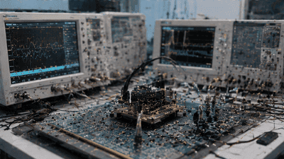
MCM simulation is hard partly because it spans multiple scales. Some phenomena happen at the nanometer or micrometer level, such as local interconnect geometry and dielectric behavior. Others happen at the package level, such as power distribution and crosstalk across chiplets. Still others happen at the system level, where board interfaces, cooling structures, and control logic come into play.
A good simulation strategy must somehow connect these scales without becoming too slow to use. That is a major challenge. Full electromagnetic simulation of a complete package can be extremely accurate, but also computationally expensive. Simplified models can be faster, but may miss critical interactions. Designers therefore need a hybrid workflow that uses detailed models where precision matters and compact models where broader exploration is needed.
This is one reason the tools for MCM analysis are evolving so quickly. The industry needs simulation that is not only accurate, but practical enough to support design iteration.
The Importance of Early Co-Design
A recurring lesson in advanced packaging is that simulation problems are easier to solve earlier in the design process. If power and signal integrity are considered only after the package architecture is fixed, the available options may be limited. Early co-design between chip, package, and board teams gives more room to adjust die placement, power grid structure, decoupling strategy, and channel topology.
In MCMs, that early planning is especially valuable because the package may be the only place where the architecture can still be adjusted without redesigning the whole product. If the team understands the power and signal requirements before tape-out, it can make better choices about:
- Where to place high-switching dies relative to sensitive ones.
- How to distribute power and ground connections.
- Which interfaces need the shortest paths and cleanest returns.
- How to balance thermal and electrical constraints in the stack-up.
That is the practical side of simulation. It is not just about predicting failure. It is about avoiding bad architectural choices before they become expensive.
Thermal Effects Are Never Far Away
Although this discussion is centered on power and signal integrity, thermal behavior is always lurking in the background. Heat changes resistance, mobility, and timing. It can alter the impedance of traces and the performance of power delivery networks. It can also cause package warpage, which in turn changes the geometry that the electrical models rely on.
That means thermal simulation must often be coupled into the PI/SI flow. A package that looks stable at room temperature may behave very differently at operating temperature. In heterogeneous integration, this matters even more because different dies may dissipate heat differently and affect each other through the package.
For this reason, advanced packaging teams increasingly treat PI, SI, and thermal as one integrated challenge rather than three separate ones. MCMs do not respect the boundaries between disciplines, so the simulation flow should not either.
Model Fidelity vs. Design Speed
One of the most frustrating trade-offs in MCM simulation is the balance between fidelity and speed. High-fidelity models capture more of the real physics, which improves confidence. But they can be slow to run and hard to use in early exploration. Lower-fidelity models are faster and easier to iterate, but they may hide critical effects until too late in the process.
Designers therefore need a staged approach. Early on, they may use compact models to compare architecture options. Later, they move to detailed electromagnetic and power integrity simulations for the most sensitive paths. At signoff, they may run full-package analysis to verify margins. This staged process is becoming standard in advanced packaging because no single model can solve the whole problem efficiently.
The challenge for simulation vendors is to support that flow without forcing engineers to rebuild their analysis from scratch at every stage.
Why Heterogeneous Integration Raises the Stakes
Heterogeneous integration is the reason PI and SI simulation in MCMs has become such a hot topic. When different functions are separated into different dies, the package has to absorb the complexity that used to live on one monolithic chip. That means more interfaces, more shared resources, and more opportunities for noise and coupling.
It also means the package has to be more honest. A monolithic chip can hide some problems inside dense internal routing. An MCM exposes them at the package boundary. The simulation flow has to be robust enough to validate the assembled system under realistic switching, loading, and thermal conditions. That is a much harder problem, but it is also a necessary one if heterogeneous integration is to keep scaling.
Practical Ways Teams Improve Simulation
The best MCM teams do not just simulate more. They simulate smarter. That often includes:
- Using reduced-order models for early trade-off studies.
- Co-simulating power and signal paths to capture interaction effects.
- Including thermal and mechanical models for realistic package behavior.
- Validating models against silicon or package measurements as early as possible.
This kind of workflow shortens the learning loop. Instead of waiting for a failed prototype to reveal a problem, designers can refine the model and the architecture together. That reduces risk and helps advanced packaging move from custom art toward repeatable engineering.
The Road Ahead
As MCMs continue to evolve, simulation challenges will only get more complex. Packages will carry more dies, higher data rates, tighter power budgets, and more aggressive thermal demands. The models will need to become better at representing real package geometry, real material behavior, and real workload patterns.
The good news is that the industry is moving in that direction. Better tools, better models, and better cross-domain collaboration are all making advanced packaging more manageable. But the fundamental challenge remains: MCMs are systems, not just packages. Power and signal integrity must be studied as system properties, or the design will miss the behavior that matters most.
Conclusion
Power and signal integrity simulation in MCMs is difficult because MCMs are difficult. They combine multiple dies, multiple materials, and multiple disciplines inside one package. That creates new coupling effects, new parasitics, and new failure modes. Advanced packaging and heterogeneous integration do not remove these challenges; they concentrate them into a smaller, more demanding space.
The key lesson is that simulation must keep pace with integration. As packages become more complex, designers need more integrated analysis, more co-design, and more realistic multi-physics modeling. In that sense, the simulation challenge is not a side effect of advanced packaging. It is one of the central reasons advanced packaging is now a serious engineering frontier.





